Popular Keywords

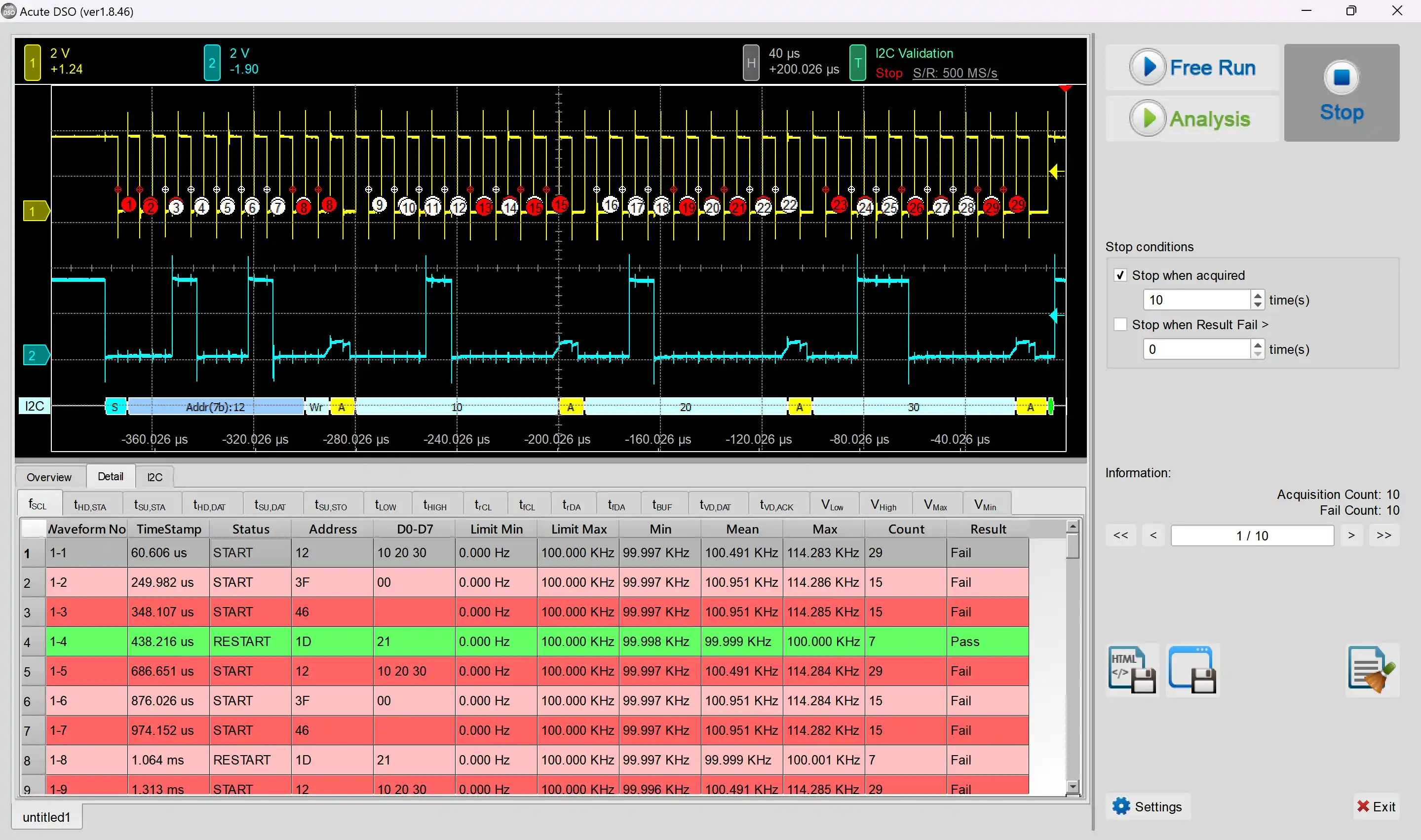
I²C Electrical Validation
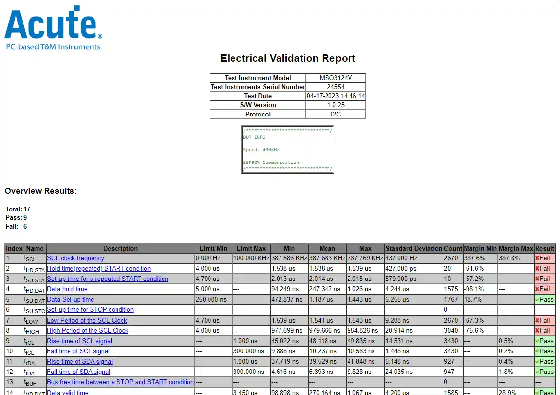
Use an oscilloscope to do I2C Electrical Validation to ensure that the I2C meets the defined specifications. It can be confirmed that the electrical characteristics of the signal to be tested meet the specifications after a long burn-in test. For protocol electrical validation

I2C Protocol electrical characteristic detection is usually divided into two types: vertical (voltage) and horizontal (time/phase).

Therefore, when using this function, you must first set the selected protocol and specifications, and then repeat the test to get the electrical characteristics test report. The test items will have different specifications and standards depending on the I2C Speed.

Supported Models:

TS3124V (4-channel DSO)

TS3124V

TS3000 Specifications PDF

TS3000 Specifications PDF

MSO3124V (4-channel DSO & 16-channel LA)

MSO3124V

MSO3000 Specifications PDF

MSO3000 Specifications PDF

Electrical Validation Solution PDF

Electrical Validation solution pdf

Overview Report

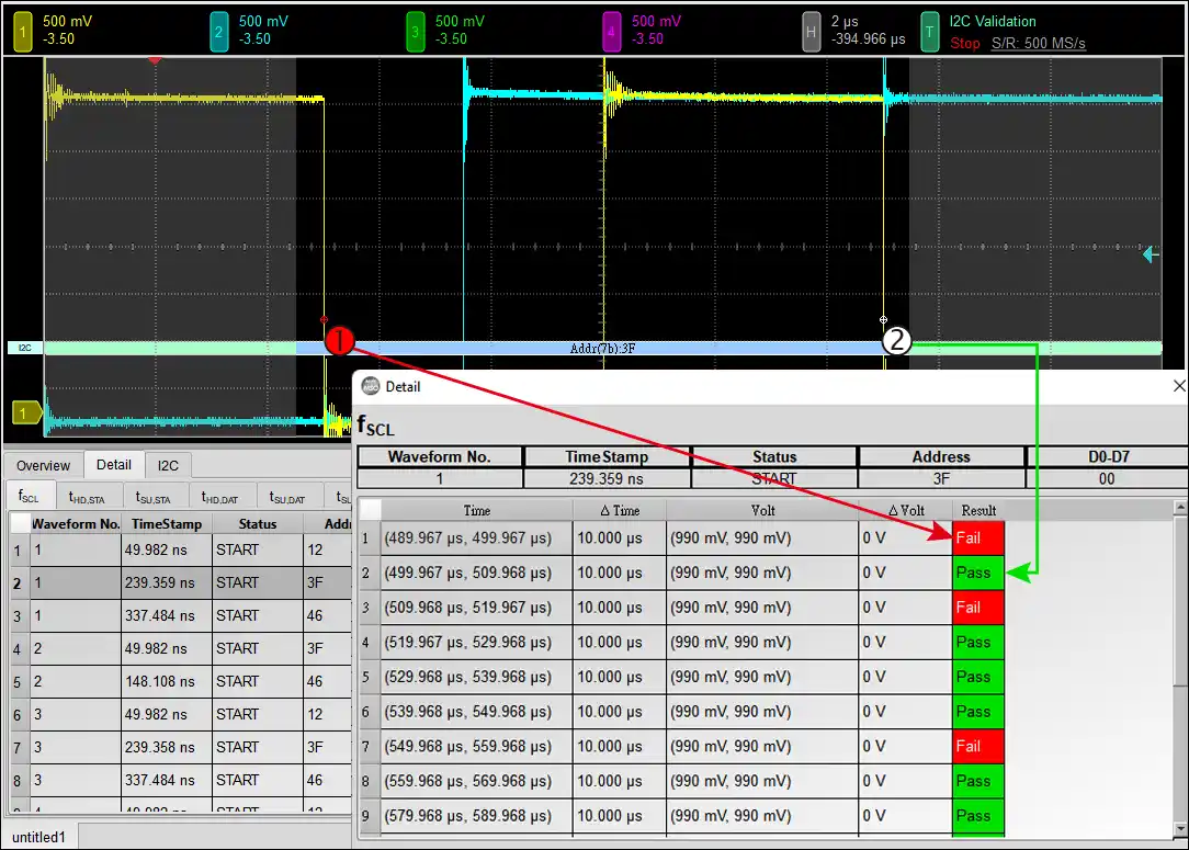
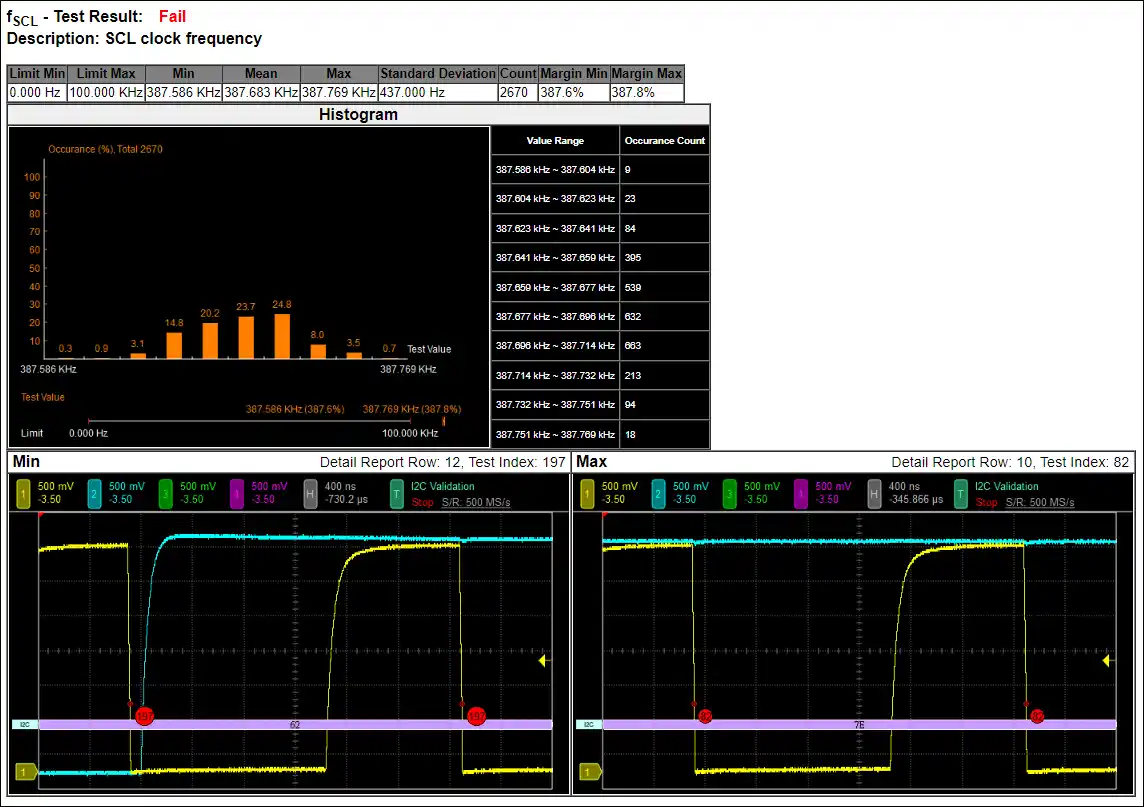
Reference Point Dialog & Waveform

HTML Report

I2C Electrical Validation Settings:

1. General Settings: Channel sources, working voltage and speed

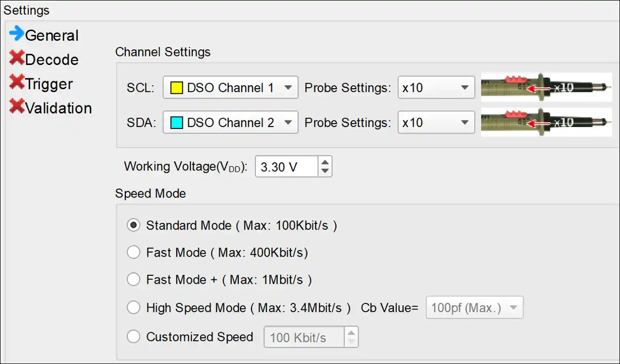
1. Different Speed Mode including Standard Speed Mode (~100kHz) / Fast Mode (~400kHz) / Fast Mode+ (~1MHz) / HS Mode(~3.4MHz)

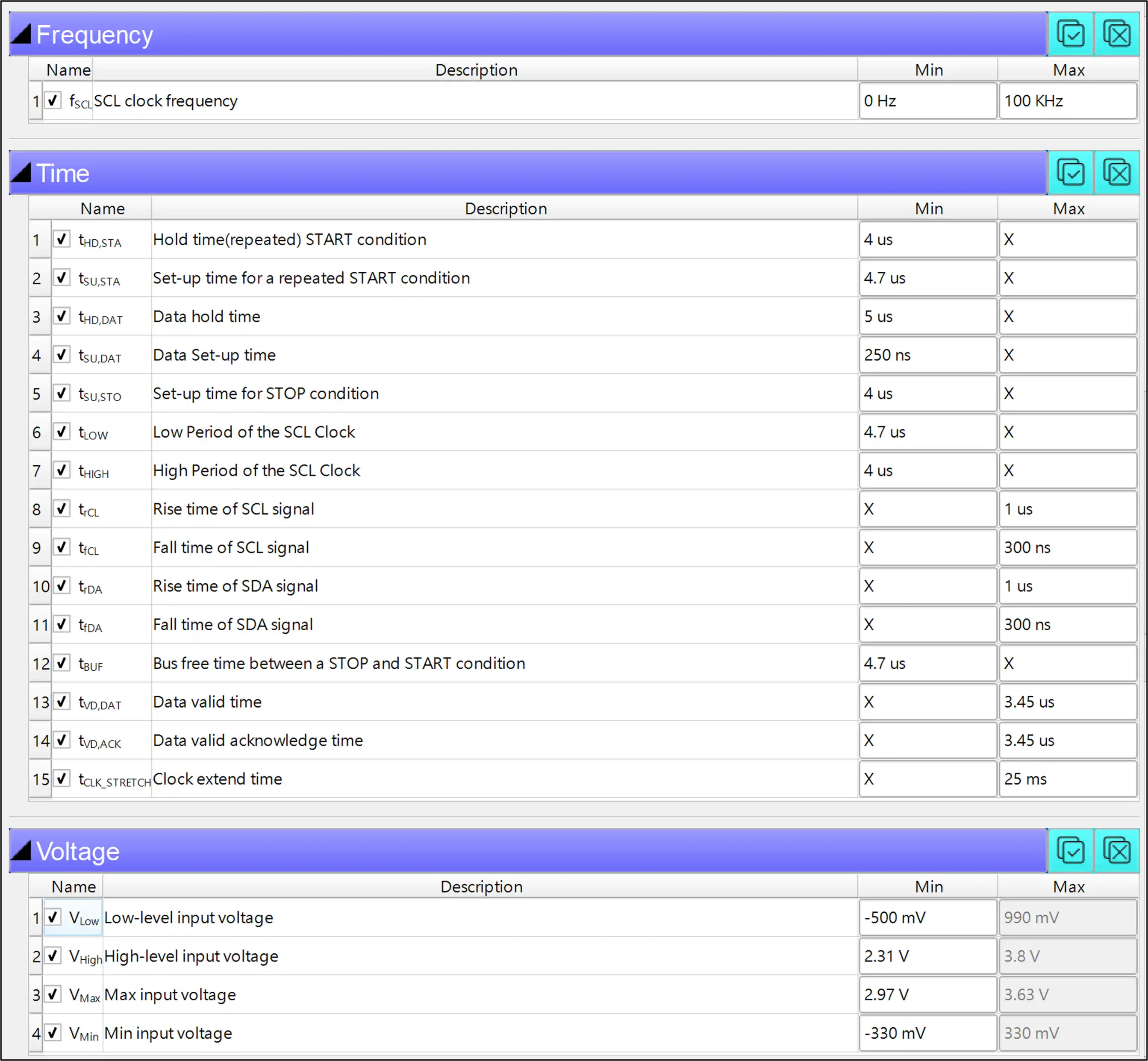
2. Frequency: Clock speed

3. Timing: Set-up Time / Hold Time / Rise Time / Fall Time & Clock Stretching Timing limitation

4. Voltage: V_IL, V_IH, etc.

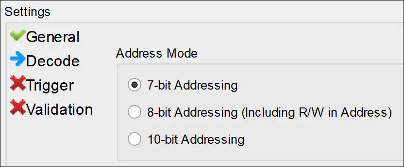
2. Decode:I2C decode settings

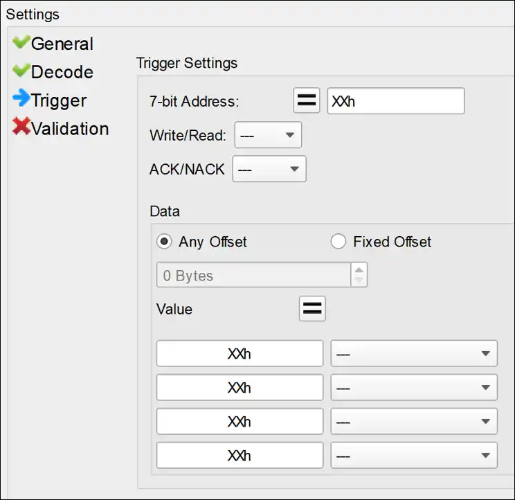
3. Trigger:I2C trigger settings


4. Electrical Validation Parameter Settings: Frequency, Timing, Voltage limitation
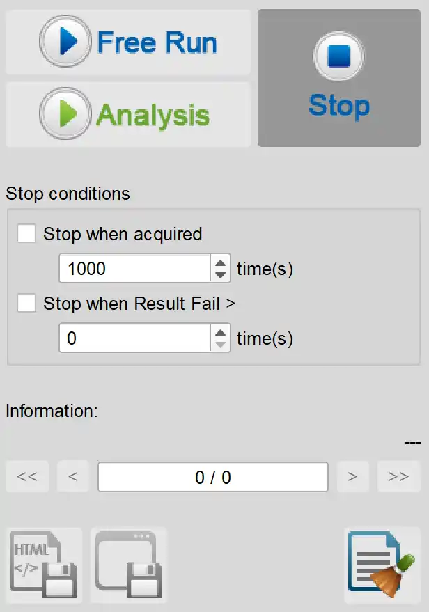
Name Description Min Max
Frequency
fSCL SCL clock frequency 0 Hz 100 KHz
Time
tHD,STA Hold time (repeated) START condition 4 µs X
tSU,STA Set-up time for a repeated START condition 4.7 µs X
tHD,DAT Data hold time 5 µs X
tSU,DAT Data set-up time 250 ns X
tSU,STO Set-up time for STOP condition 4 µs X
tLOW Low period of the SCL clock 4.7 µs X
tHIGH High period of the SCL clock 4 µs X
tRCL Rise time of SCL signal X 1 µs
tFCL Fall time of SCL signal X 300 ns
tRDA Rise time of SDA signal X 1 µs
tFDA Fall time of SDA signal X 300 ns
tBUF Bus free time between a STOP and START condition 4.7 µs X
tVD,DAT Data valid time X 3.45 µs
tVD,ACK Data valid acknowledge time X 3.45 µs
tCLK,STRETCH Clock extend time X 25 ms
Voltage
VLow Low-level input voltage -500 mV 990 mV
VHigh High-level input voltage 2.31 V 3.8 V
VMax Max input voltage 2.97 V 3.63 V
VMin Min input voltage -330 mV 330 mV

5. Software EV control panel:

Stop Conditions:
Stop when acquired X times
Stop when Result Fail > X times

Information:
Select waveform

Save File:
Save as Html
Save as .MOW (Software format)

YouTube Video

Electrical Validation Solution PDF

Electrical Validation solution pdf

We use cookies to elevate your user experience and enhance the quality of our site. To find out more or adjust cookie settings, click here .