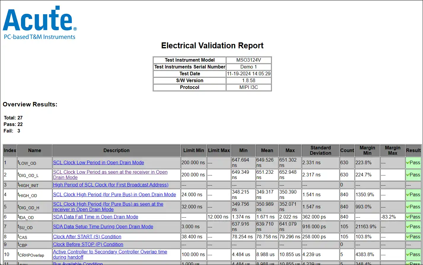
MIPI I3C Electrical Validation
Overview Report
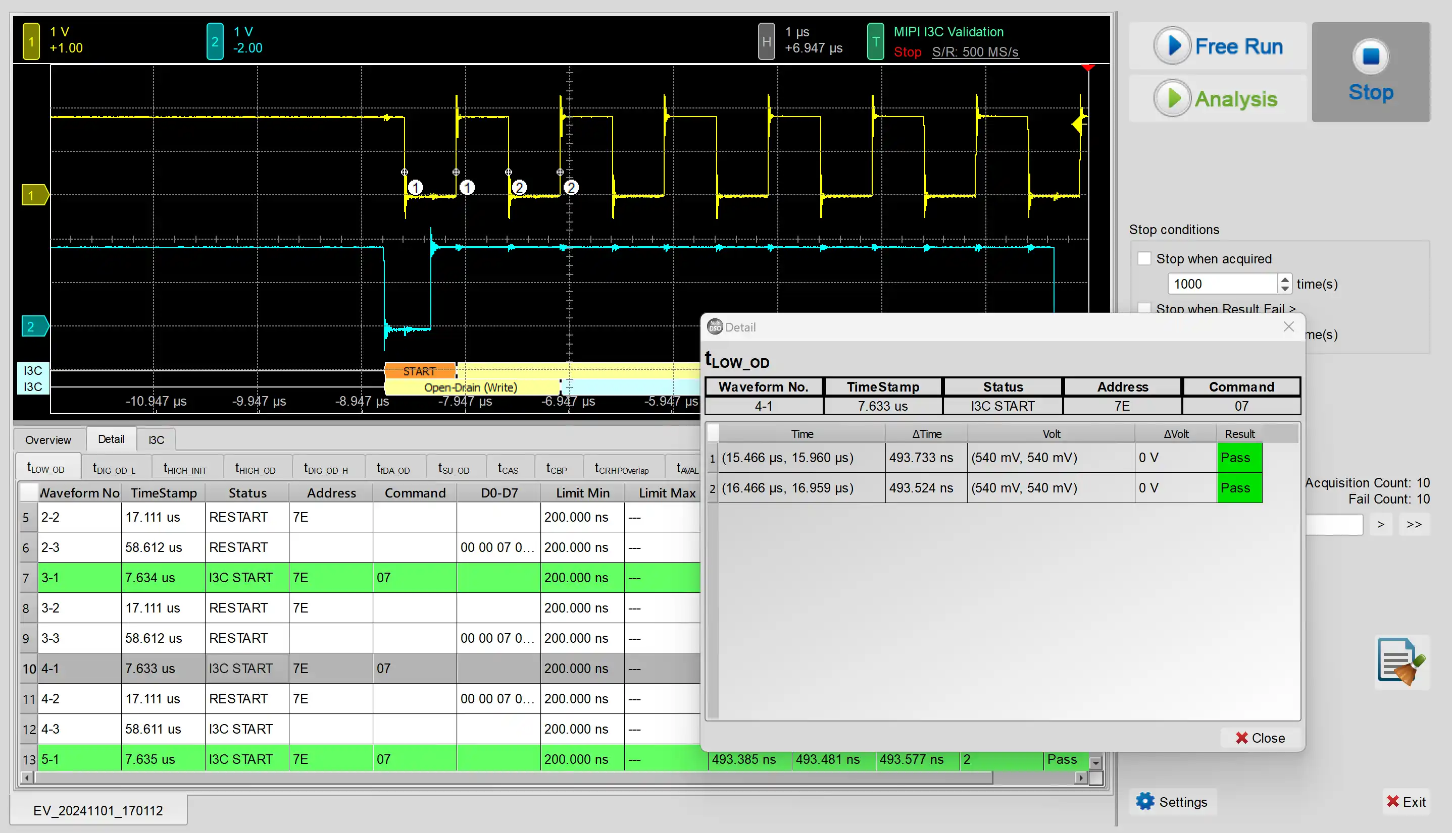
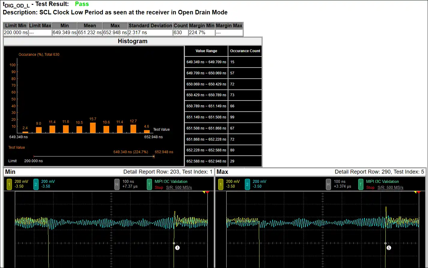
Reference Point Dialog & Waveform:
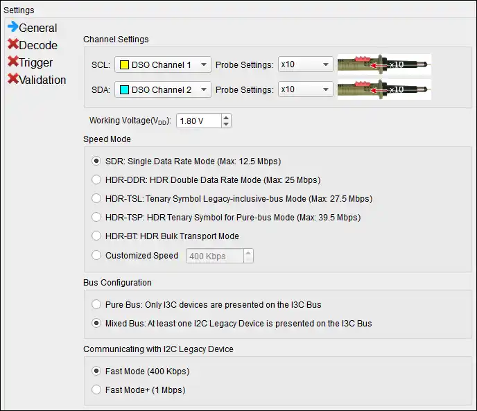
1. General Settings: Channel sources, working voltage and speed
In the General Settings section, the selection of Speed Mode determines a suitable sample rate for validation, but also affects the timing specification table in the validation settings section. For instance, in HDR-TSL and HDR-TSP Mode, there are additional timing specifications listed in the table.
Furthermore, the Bus Configuration section specifies the devices you connected on the I3C Bus. If it is a Pure-Bus setup, I2C timing table is thus not required, which is discussed in the Validation Settings section. On the other hand, a Mixed Bus setup will include the timing table for I2C Legacy Devices, and there default timing values are determined by using Fast Mode (Fm) or Fast Mode (Fm+) configuration, which is an identical settings to I2C Electrical Validation setup.
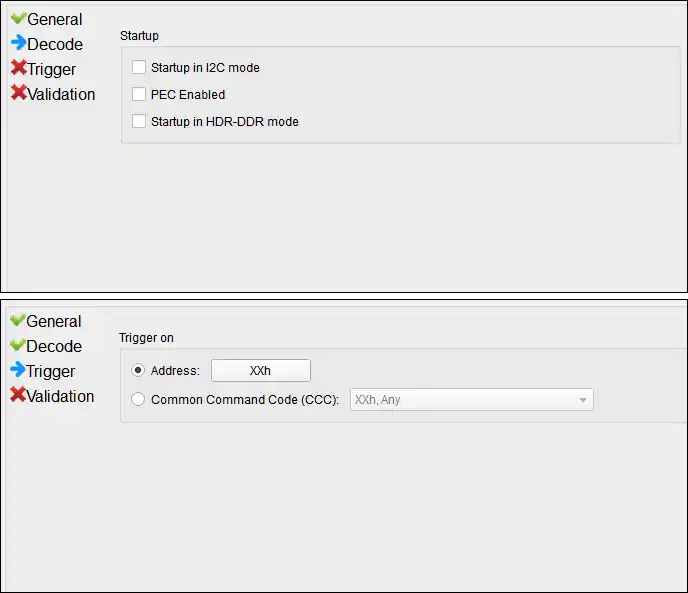
2~3. Decode / Trigger Settings:
If you are interested in analyzing specific devices address, set the trigger address to the value you prefer. In the figure above, “XX” stands for don’t care term. Thus, it triggers on all address in this case. It also provides triggering on Common Command Code (CCC), which is specified on the Broadcast Address 7’h7E.
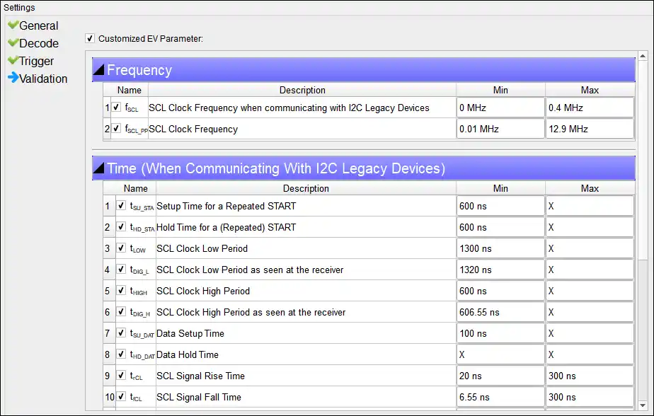
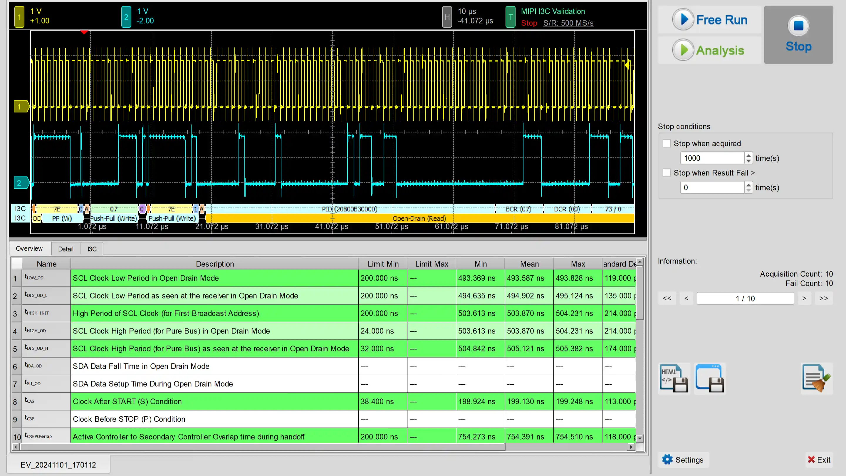
This section includes 5 parameter tables, including
• Frequency
• I3C timing requirements when communicating with I2C Legacy Devices
• I3C Open Drain timing parameters
• I3C Push-Pull timing parameters
• I3C I/O stage characteristics voltage requirements
In the Pure Bus setup, the timing requirements table with I2C Legacy Devices is not required and thus be hidden from the parameter settings dialog. The frequency parameter fSCL will also be hidden in the Pure Bus setup.
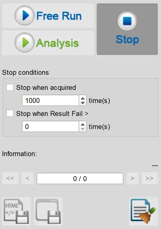
Stop Conditions:
Stop when acquired X times
Stop when Result Fail > X times
Information:
Select waveform
Save File:
Save as Html
Save as .MOW (Software format)
Electrical Validation Solution PDF