JTAG
JTAG (Joint Test Action Group) stands as an international standard testing protocol (IEEE 1149.1), primarily employed for internal testing of various chips, including CPU, DSP, CPLD, FPGA, and more. Initially developed by the Joint Test Action Group organization, it later evolved into the widely adopted IEEE 1149.1 standard, playing a crucial role in electronic design and manufacturing.
The JTAG standard incorporates five signal interfaces: TCK, TMS, TDI, TDO, and TRST. Four of these interfaces are designated for input signals, while the remaining one serves as an output signal interface. Originally conceived for chip testing, JTAG establishes a Test Access Port (TAP) within the component, facilitating the testing of internal nodes through dedicated JTAG testing tools.
Within the JTAG standard, a typical voltage range of 5V is utilized. This voltage design ensures sufficient signal amplitude, guaranteeing reliability during JTAG communication. However, technological advancements have introduced applications employing lower voltages, such as 1.8V or 3.3V, to align with the demands for low power consumption and modern chip design.
Logic Analyzer
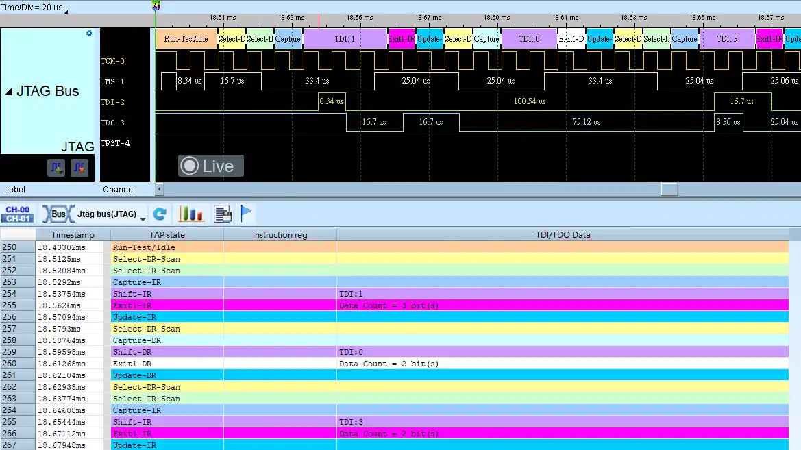
JTAG Decode
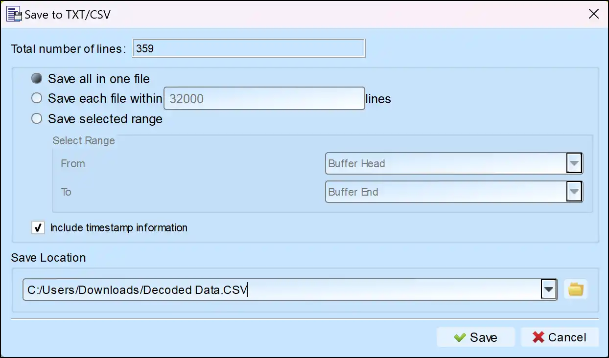
Save as TXT/CSV
In Logic Analyzer mode, click the icon above the report area to save the decoded data as a TXT/CSV file.

JTAG Decoding Setup Steps
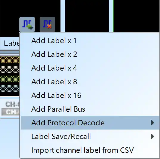
1. Click Quick Settings or Add Protocol Decode to select a protocol for logic analyzer capture.
2. Select JTAG for decoding.
3. If you use Quick Settings, the system will recommend configurations for trigger type, sampling rate, voltage threshold, and channel settings.
4. Click the icon to access the Decode Settings screen.


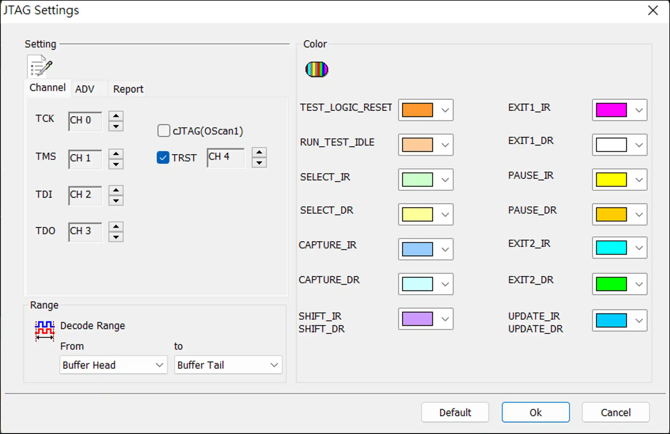
Decode Settings
Channel: Set the channel number.
cJTAG: Once enabled, TDI/TDO will be presented in gray, and TCK/TMS will be the TCKC/TMSC channel in cJTAG (OScan1) mode.
TRST: If the interpret command function is available, the system will decide whether to use the TRST pin based on the command data you selected.
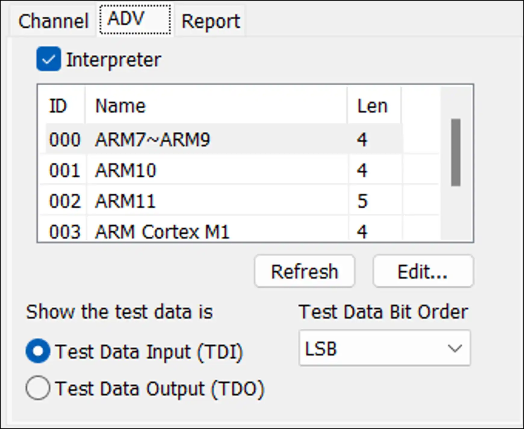
ADV Settings
Interpreter: Enable the Interpreter Instruction section to find a comprehensive list of commands. The JTAG decode will showcase the latest commands in the Instruction Register, serving as a temporary memory buffer. To modify the commands within the Interpreter Instructions, select Edit, and subsequently, click Refresh to ensure the updates are applied to the Interpreter Instructions.
Test data: Select Input (TDI) or Output (TDO); the TDI or TDO data will be displayed in hexadecimal.
Test data bit order: Due to JTAG data transmission, the data length may be variable. Therefore, the user can specify whether the data is LSB First or MSB First when interpreting TDI/TDO.
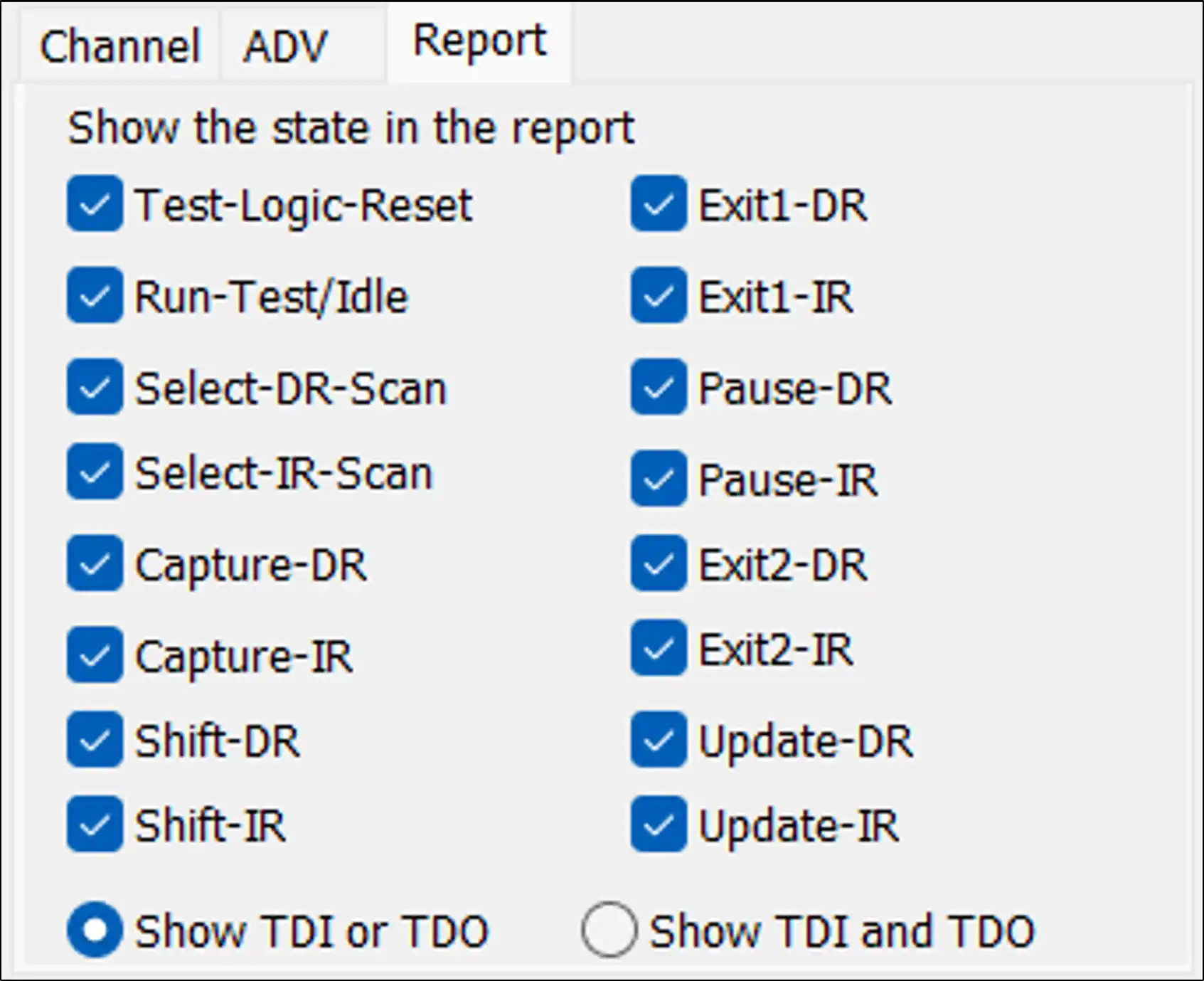
Report Settings
Report: You can filter the data you want to see on the Report Window.
Show TDI or/and TDO: Show either TDI or TDO or both.
