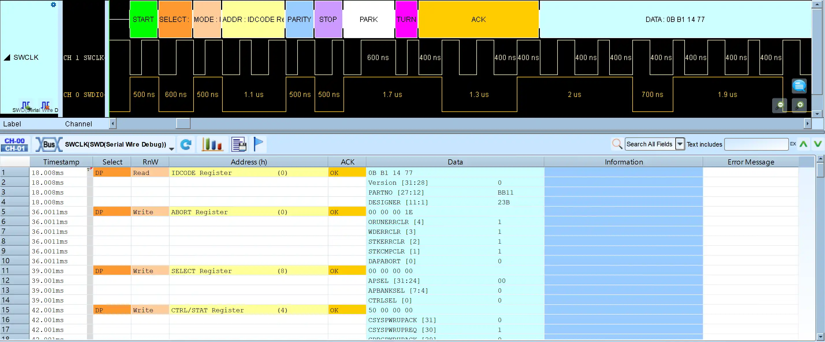
SWD (Serial Wire Debug)
SWD Decode
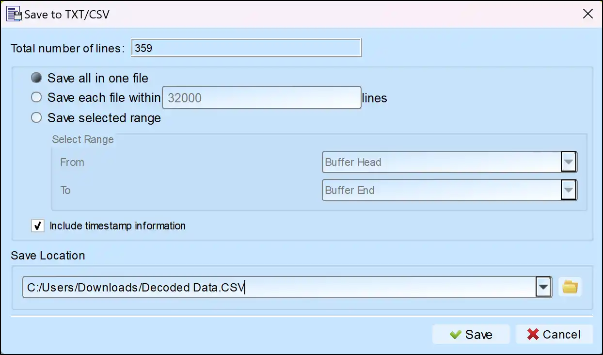
Save as TXT/CSV
In Logic Analyzer mode, click the icon above the report area to save the decoded data as a TXT/CSV file.

SWD Decoding Setup Steps
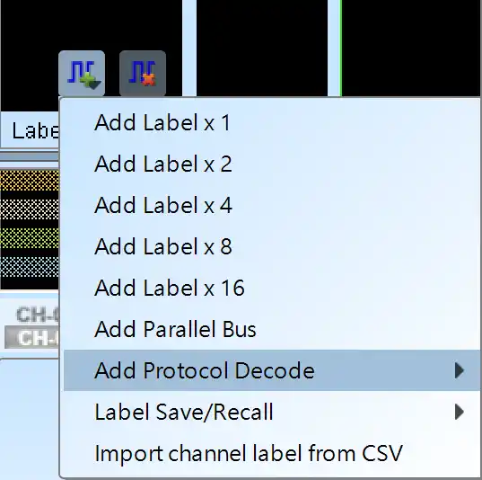
1. Click Quick Settings or Add Protocol Decode to select a protocol for logic analyzer capture.
2. Select SWD(Serial Wire Debug) for decoding.
3. If you use Quick Settings, the system will recommend configurations for trigger type, sampling rate, voltage threshold, and channel settings.
4. Click the icon to access the Decode Settings screen.

SWDIO: I/O data.
SWDCLK: Clock.
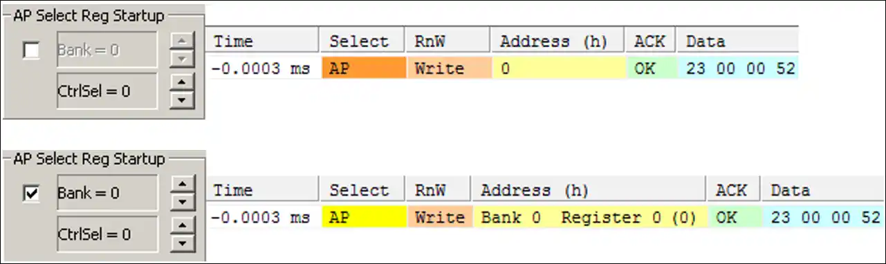
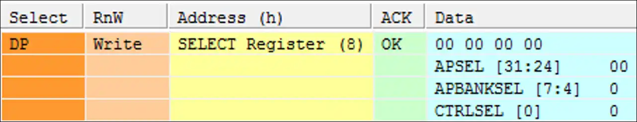
AP Select Reg Startup
Bit Order: LSB or MSB.
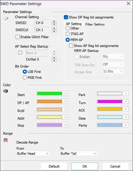
Show DP Reg bit assignments: Show the DP register information.
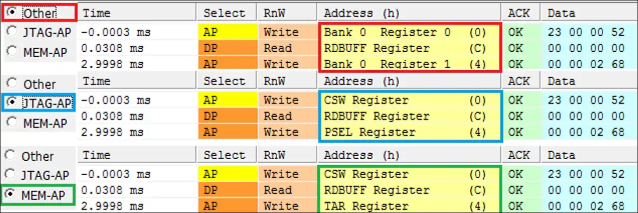
AP Setting: You can select between MEM-AP and JTAG-AP for AP Register decoding. If the user selects Other, the AP data will only display as Bank X Register X without further interpretation.
Other: Show Bank X Register X.
JTAG-AP: Show the JTAG AP decode.
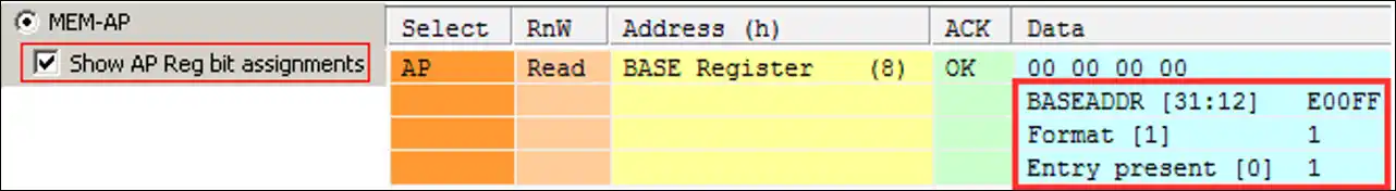
MEM-AP: Show the MEM AP decode.
Show AP Reg bit assignments: Display the AP register information if JTAG-AP or MEM-AP checked.
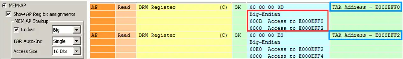
MEM AP Startup: When selecting MEM-AP, the contents of MEM-AP can be initialized. During data capture, if a corresponding register address is encountered, the data will be updated according to the bus content. Enabling the Endian checkbox activates the display of data along with the corresponding read/write addresses.
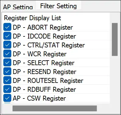
Filter Setting: Filter the unwanted Registers.
SWD Decoding Examples