I3C 电气特性验证 Electrical Validation
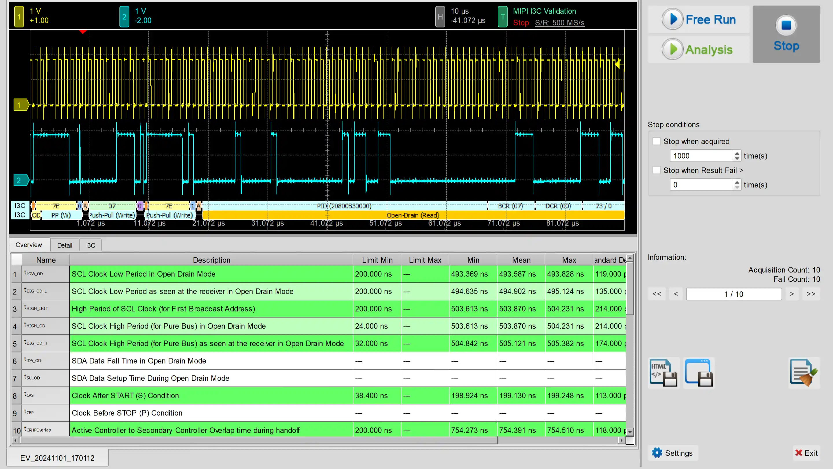
电气特性验证 软件画面
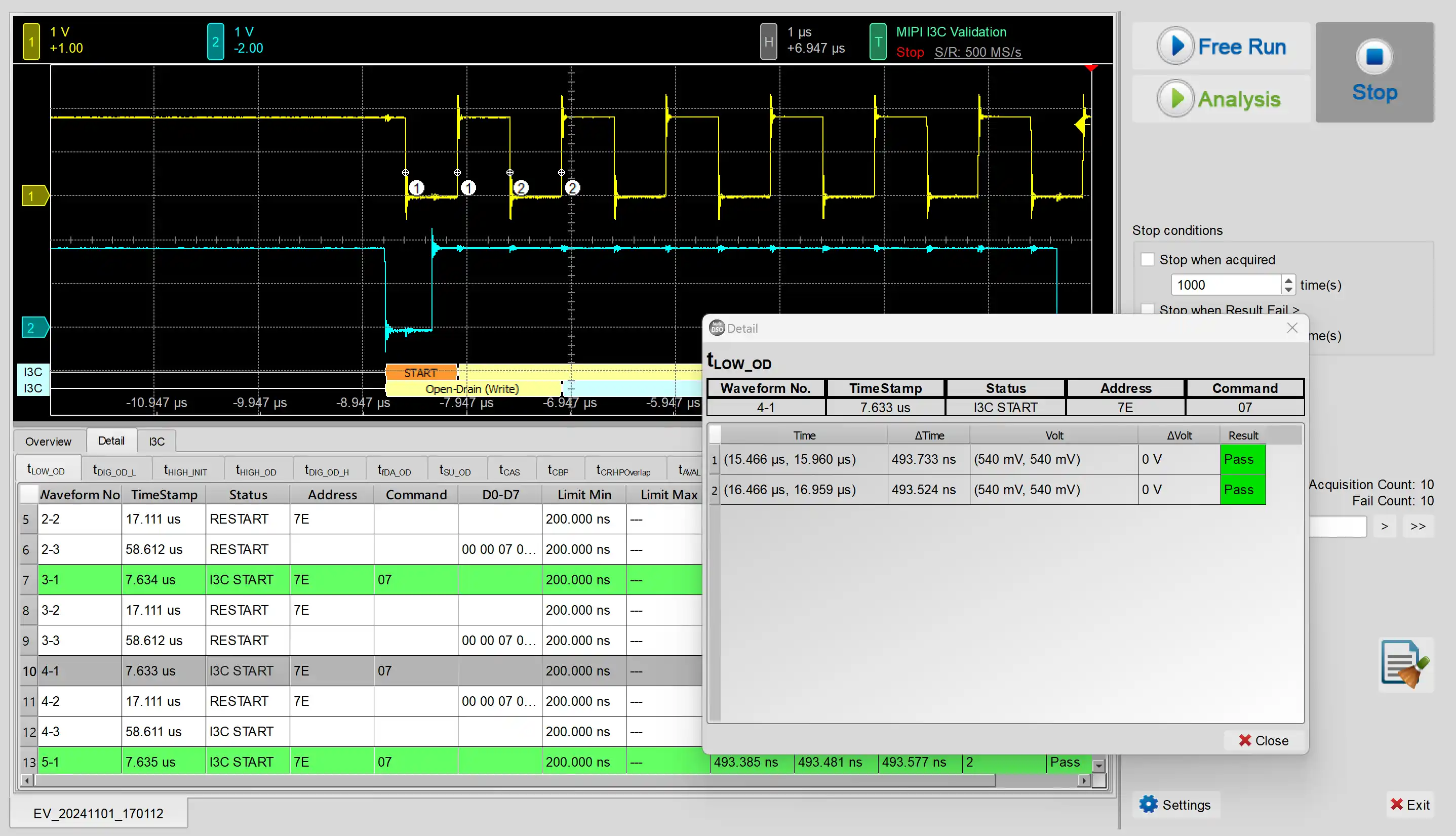
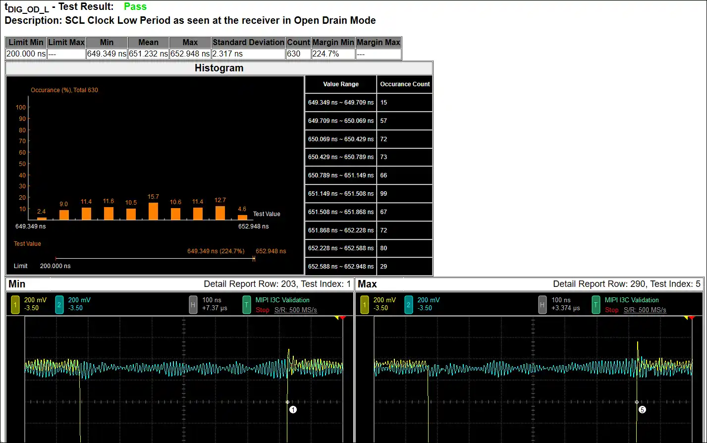
波形和参考点
HTML 报告总表 - 有对应连结,可方便输出/查询/传递
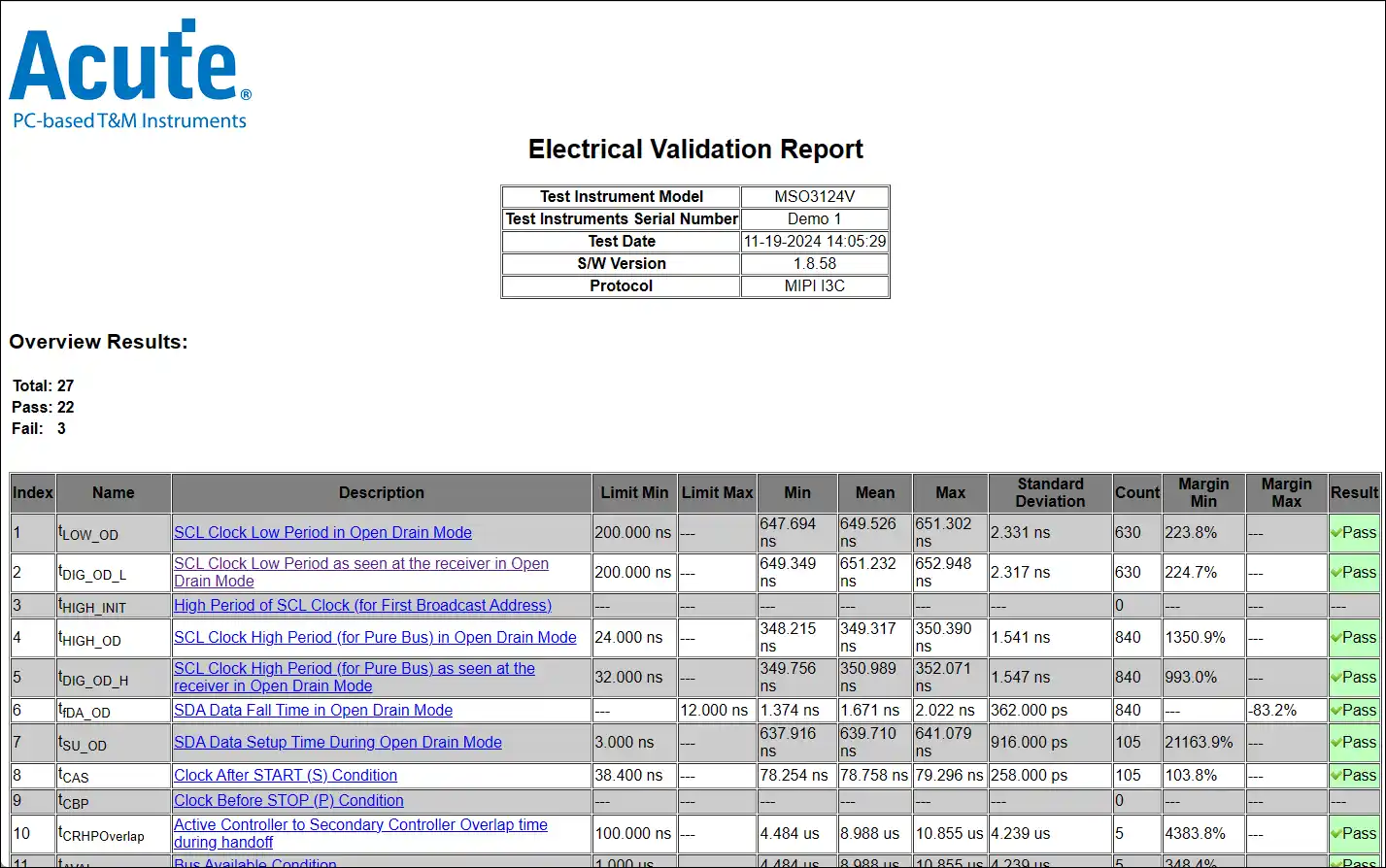
HTML报告 详细内容
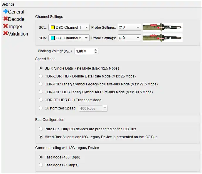
1. 一般设置:通道来源、工作电压与速度
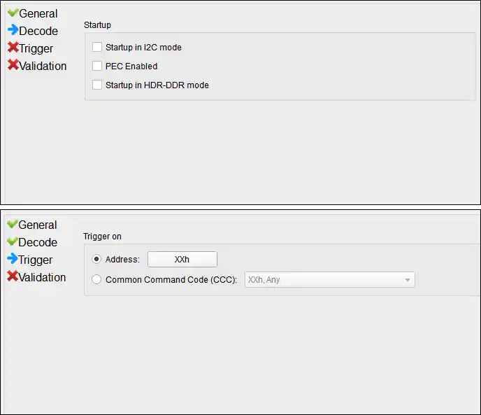
2~3. Decode / Trigger:I3C 解码 / 触发 设置
4. 验证参数设置:频率、时序与电压限制条件
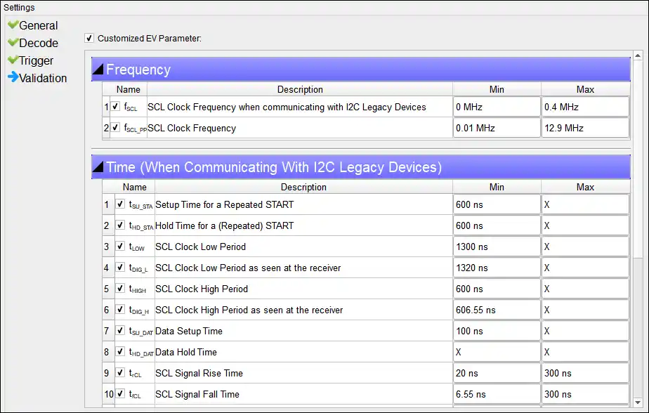
本部分共包含五种参数表:
• Frequency
• I3C timing requirements when communicating with I2C Legacy Devices
• I3C Open Drain timing parameters
• I3C Push-Pull timing parameters
• I3C I/O stage characteristics voltage requirements
若为纯 I3C 总线,则不会显示与 I2C 装置相关的时序表,也不会显示 fSCL 频率参数。
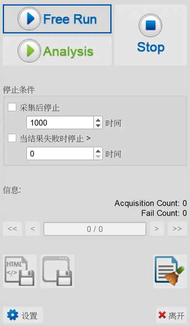
停止条件:
当采集达到 X 次时停止
当测试结果失败超过 X 次时停止
信息:
选择查看波形
储存档案:
储存为 HTML 格式
储存为 .MOW(Acute软件专用格式)
电气特性验证 方案说明 PDF